CMP & BONDING FOUNDRY
CMP Foundry Service|Bonding Foundry Service
CMP Foundry Service|Bonding Foundry Service


D-process provides integrated Foundry service services focused on CMP Foundry service and bonding Foundry service for prototyping/development and mass production of various electronic devices.
●Processing offered by D-process
・Procurement of various wafers
・Insulation layer formation by various film formation methods (SiO2, CVD, TEOS, etc.)
・Mask production and patterning (wet etching/dry etching, etc.)
・Barrier metal formation (Ta, TaN, Ti, TiN, Cr, etc.)
・Seed layer formation by sputtering, deposition, and electroless plating to plating processing such as for Cu, Au, Ni, etc.
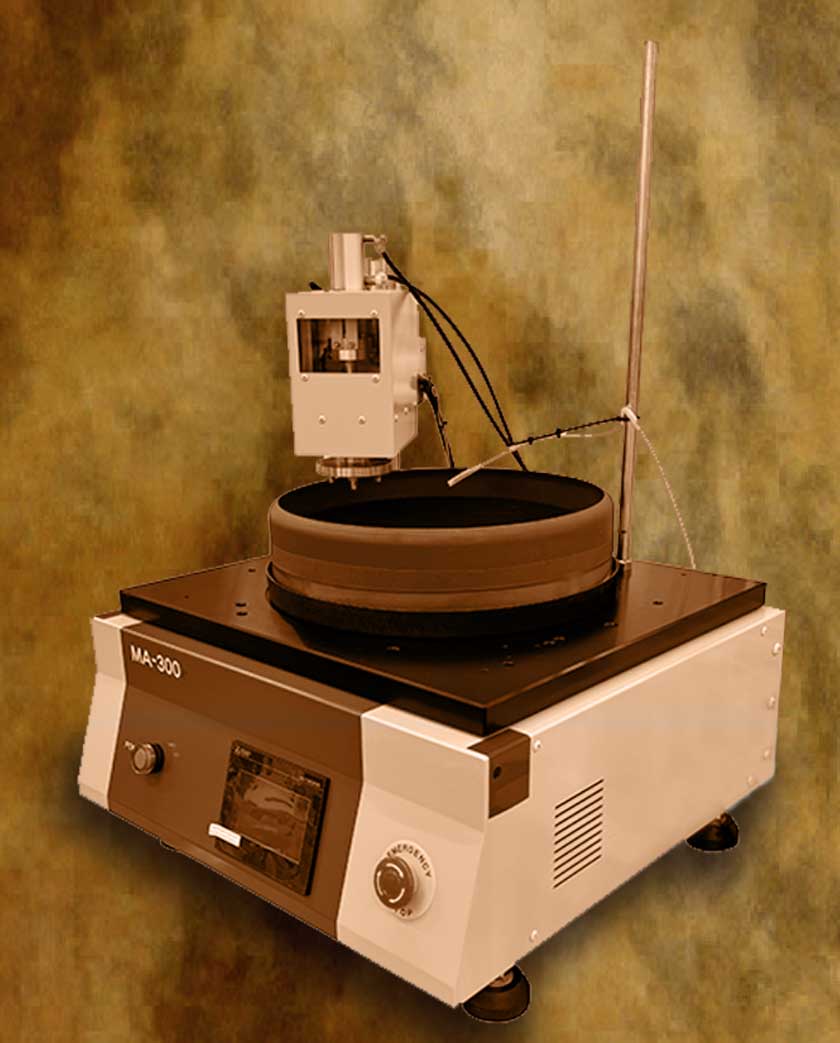
・Planarization by CMP contract processing
・Wafer bonding contract processing after CMP wafer pre-processing (room temperature bonding, plasma-activated bonding, diffusion bonding, eutectic bonding, resin bonding, temporary bonding/debonding)
・Edge processing such as terrace processing and trimming processing
・Backside grinding - Thinning by CMP
・Conversion into small pieces by dicing
・Quality assurance by various measuring instruments such as AFM, profilometer, film thickness gauge, thickness gauge, SEM, ultrasonic microscope (C-SAM), IR, etc.
The CMP process has developed as a part of the LSI manufacturing process, but in recent years it has begun to be widely applied in other fields.
In semiconductor manufacturing, the CMP process was originally applied to the lithography process to meet depth of focus requirements or to planarization of embedded wiring. On the other hand, the CMP process has begun to be applied in fields focusing on MEMS and power devices (mainly pre-bonding processing including room temperature bonding). D-process's CMP contract processing enables everything from prototyping/development to volume production in such application fields. We guarantee planarization for materials and applications that require flattening, regardless of the boundaries of LSI, MEMS, power devices, communication devices, and optical devices.
For contracted bonding processing on the other hand, we have introduced state-of-the-art bonding equipment to support all applications.
In addition to room temperature bonding, plasma-activated bonding, diffusion bonding, eutectic bonding, and temporary bonding/debonding (TB/DB) by resin bonding are also supported, and prototyping/development to production/mass production are possible.
With popular demand in recent years for 3D mounting such as HBM, D-process has also made efforts to establish a process for C2W bonding Foundry service.
D-process's unique C2W bonding Foundry service utilizes technology cultivated through direct wafer bonding such as room temperature bonding and plasma-activated bonding to handle everything from prototyping/development to production/mass production.
Wafer direct bonding and C2W bonding by D-process achieves void-free, high-quality bonding through CMP pre-processing using our unique slurry, and quality is ensured by the use of an ultrasonic microscope (C-SAM) and IR camera.
At D-process, we will strive daily to improve our technical capabilities as a frontrunner of CMP and bonding Foundry service.